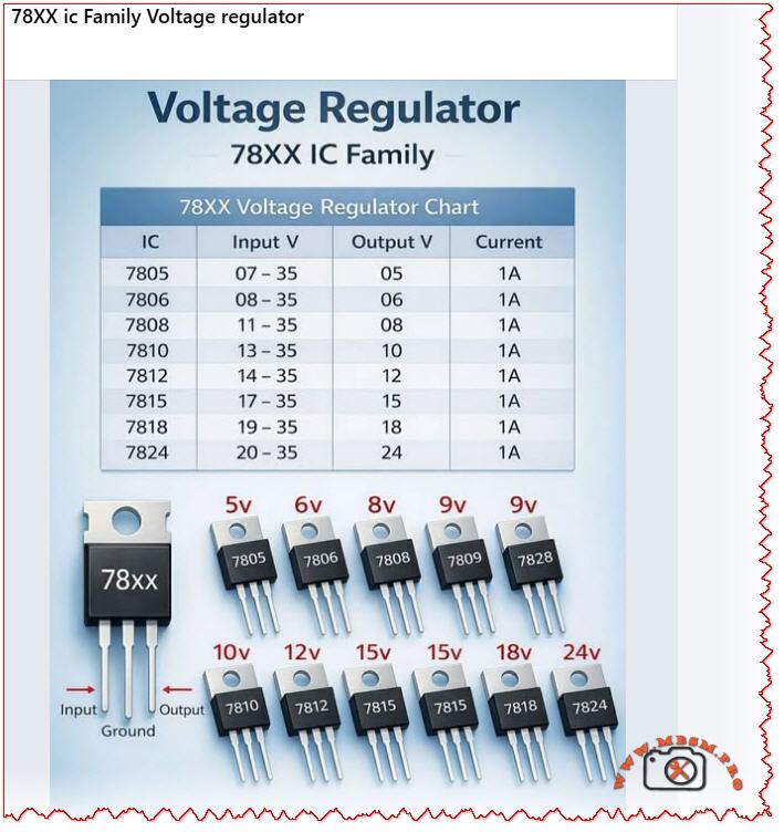
78XX IC Family, Voltage Regulator
Mbsmpro.com, 78XX IC Family, Voltage Regulator, 7805, 7806, 7808, 7810, 7812, 7815, 7818, 7824, 5V, 6V, 12V, 15V, 24V, Linear Regulator, 1.5A, Thermal Protection
78XX Voltage Regulator Family: Complete Technical Guide & Applications
The 78XX series is one of the most widely adopted family of linear voltage regulators in electronics. These three-terminal ICs have powered countless consumer devices, industrial systems, and hobbyist projects since their introduction decades ago. From a simple 5V supply for microcontrollers to a robust 24V rail for automation, the 78XX family delivers fixed regulated voltage with minimal external components.
Whether you are designing a power supply, troubleshooting an embedded system, or maintaining legacy equipment, understanding the 78XX lineup—including the 7805, 7812, 7815, 7824, and their companions—is essential knowledge.
What Is the 78XX Voltage Regulator?
A voltage regulator is an electronic component that maintains a constant output voltage despite fluctuations in the input supply or changes in the load current. The 78XX family does this using a linear approach: it essentially acts as an intelligent resistor, dropping excess input voltage while supplying current at the regulated output level.
The “78XX” designation is a naming convention:
- “78” indicates a positive voltage regulator (as opposed to 79XX for negative regulators).
- “XX” is replaced by two digits representing the output voltage.
For example:
- 7805 = 5 V output
- 7812 = 12 V output
- 7824 = 24 V output
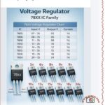
Complete 78XX Series Specifications & Voltage Breakdown
Below is the definitive reference table for the standard 78XX family, showing all available output voltages, input requirements, and current capability.
| IC Model | Output Voltage (V) | Min Input Voltage (V) | Max Input Voltage (V) | Typical Output Current (A) | Package | Typical Application |
|---|---|---|---|---|---|---|
| 7805 | 5.0 | 7.0 | 25 | 1.5 | TO-220, TO-3 | Microcontroller, logic circuits, SPI devices |
| 7806 | 6.0 | 8.5 | 25 | 1.5 | TO-220 | Audio preamplifier, sensor supply |
| 7808 | 8.0 | 10.5 | 25 | 1.5 | TO-220 | Industrial sensor supply, panel meters |
| 7810 | 10.0 | 12.5 | 28 | 1.5 | TO-220 | Analog circuits, operational amplifier supply |
| 7812 | 12.0 | 14.5 | 30 | 1.5 | TO-220, TO-3 | Automotive applications, motor logic control |
| 7815 | 15.0 | 17.5 | 30 | 1.5 | TO-220, TO-3 | Industrial automation, TTL logic systems |
| 7818 | 18.0 | 20.0 | 35 | 1.5 | TO-220 | Audio amplifier supplies, high-voltage relay logic |
| 7824 | 24.0 | 27.0 | 38 | 1.5 | TO-220, TO-3 | Solenoid driver supplies, PLCs, high-power circuits |
Key observations:
- Output voltage range spans from 5 V to 24 V, covering nearly all common digital and analog supply voltages.
- Input voltage must exceed output by at least 2–3 V (called the dropout voltage). For example, the 7805 requires minimum 7 V input to reliably deliver 5 V.
- All variants provide up to 1.5 A continuous output current, making them suitable for moderate-power applications.
- Larger output voltages (7815, 7824) allow higher maximum input voltage, useful in industrial environments.
78XX Internal Architecture & Operating Principle
The 78XX IC is a monolithic linear regulator, meaning all components are integrated on a single silicon die. Here is how it works internally:
Functional Block Diagram (Conceptual)
text┌─────────────────────────────────────────────────────────┐
│                    78XX Voltage Regulator               │
│                                                         │
│  Input  ──┬─→ [Reference      ┌──→ [Error Amp]       │
│  (Vin)    │    Voltage Diode]  │    Comparator     Output
│           │    ~ 1.25V         │    & Driver    ┬──→ (Vout)
│           │                    │                │
│  Ground ──┴────────────────────┴────────────────┴─→ (GND)
│           │                                     │
│           └─ [Pass Transistor (Darlington)]────┘
│           │    Current Limiting & Thermal      │
│           │    Protection Circuit              │
│           └──────────────────────────────────────┘
│                                                         │
└─────────────────────────────────────────────────────────┘
How it regulates:
- Reference Voltage: An internal Zener diode generates a stable ~1.25 V reference.
- Error Amplifier: Continuously compares the output voltage (via a voltage divider) against the reference.
- Pass Transistor: A high-power Darlington transistor acts as a dynamic resistor, adjusting its resistance to maintain constant output voltage.
- Feedback Loop: If output voltage rises, the error amp reduces pass transistor conductance (increases resistance). If output falls, it increases conductance. This negative feedback keeps output voltage rock-steady.
Built-in protection circuits:
- Current Limiting: If load current exceeds ~2.2 A (typical), internal circuitry reduces the pass transistor bias, preventing damage.
- Thermal Shutdown: If junction temperature exceeds ~125 °C, the regulator shuts down until cooling.
- Short-Circuit Protection: If output is shorted to ground, the current limiter engages immediately.
78XX Device Comparison: Series-by-Series Breakdown
Understanding the differences and similarities helps you choose the right device for your design.
78XX vs. 79XX (Negative Regulators)
| Feature | 78XX (Positive) | 79XX (Negative) |
|---|---|---|
| Output polarity | Positive voltage | Negative voltage |
| Ground reference | Ground is 0 V | Ground is 0 V, output below ground |
| Typical use | Most digital logic, microcontroller power | Dual-supply op-amp circuits, symmetrical supplies |
| Pin configuration | IN / GND / OUT (left to right) | IN / GND / OUT (same order) |
| Examples | 7805 (5V), 7812 (12V) | 7905 (−5V), 7912 (−12V) |
78XX vs. LM317 (Adjustable Regulator)
| Aspect | 78XX (Fixed) | LM317 (Adjustable) |
|---|---|---|
| Output voltage | Fixed (e.g., 5V, 12V) | User-adjustable via resistor divider |
| External parts | Minimal (2 capacitors) | More components (2 resistors + 2 capacitors) |
| Design flexibility | Low; choose IC for desired voltage | High; one IC, many output voltages |
| Design complexity | Beginner-friendly | Intermediate |
| Quiescent current | ~3–5 mA | ~3–5 mA |
| Max output current | 1.5 A (1 A for 78L variant) | 1.5 A (higher for LM350/LM338) |
Physical Packages: TO-220 vs. TO-3
The 78XX is available in different packages, each suited to specific thermal and space constraints.
TO-220 Package (Most Common)
- Dimensions: Roughly 10 mm × 5 mm × 5 mm tall.
- Pins: Three leads (IN, GND, OUT).
- Mounting: Can be soldered to PCB directly or mounted on a small heatsink.
- Thermal resistance (package only): ~50–65 °C/W (case to ambient without heatsink).
- Best for: General-purpose designs, moderate power dissipation (<2 W).
TO-3 Package (High-Power)
- Dimensions: Larger, roughly 25 mm × 10 mm.
- Mounting tab: Large metal collector tab for heatsink mounting (provides excellent thermal path).
- Thermal resistance (with heatsink): ~1–2 °C/W (when mounted on large finned heatsink).
- Best for: Industrial applications, sustained high current (approaching 1.5 A), harsh environments.
Field note: A 7805 in TO-220 without a heatsink can dissipate only ~500 mW before overheating. The same IC in TO-3 with a proper heatsink can safely handle 10+ watts of continuous dissipation.
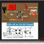
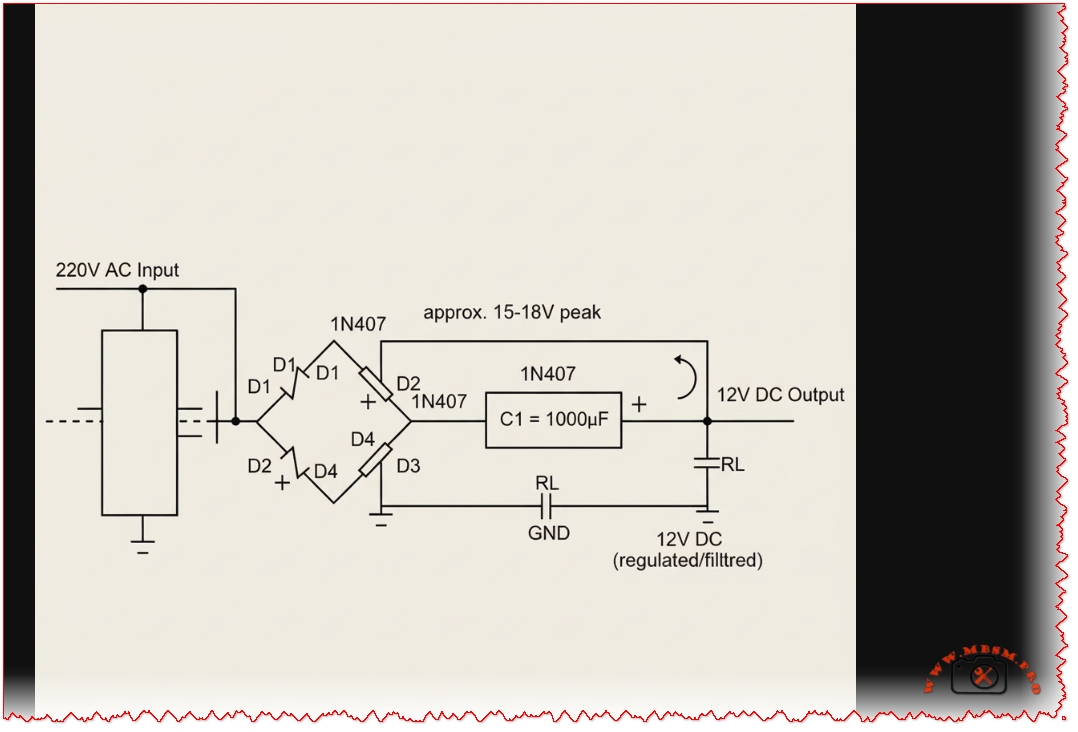
Step-by-Step: How to Design a Simple 78XX Power Supply
Example: 12V / 1.5A Regulated Supply Using 7812
Components needed:
| Component | Value | Purpose |
|---|---|---|
| Transformer (T1) | 18 VAC, 2 A | Step down mains voltage |
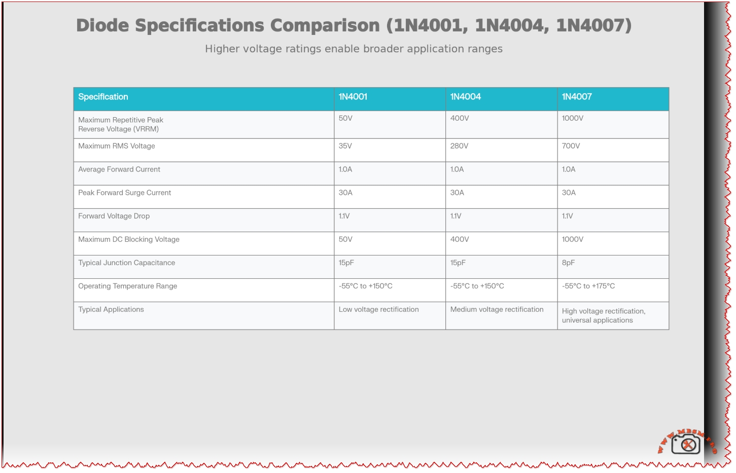
| Bridge Rectifier (D1–D4) | 1N4007 (or 1N4004) × 4, or bridge module | Convert AC to pulsating DC |
| Filter Capacitor (C1) | 2200 µF, 35 V (electrolytic) | Smooth rectified voltage |
| Input Bypass (C2) | 0.33 µF ceramic | Reduce high-frequency noise at 7812 input |
| Output Bypass (C3) | 0.1 µF ceramic | Reduce output ripple |
| IC1 | LM7812 (or 7812 variant) | Voltage regulator |
| Heatsink | Aluminum fin, ~1 K/W | Thermal management for 7812 |
| Output LED (optional) | 5 mm red LED + 1 kΩ resistor | Power indicator |
| Fuse (F1) | 2 A slow-blow | Protection |
Circuit Operation:
- AC Input (18 VAC): From transformer secondary.
- Rectification: Bridge diode converts AC to ~25 VDC (peak), with ripple.
- Filtering: Large capacitor (2200 µF) smooths to ~20–22 VDC steady-state (ripple ~2–3 V).
- Regulation: LM7812 inputs 20–22 VDC, outputs stable 12.0 VDC.
- Output: Clean 12 V can power logic, relays, or motors.
Thermal calculation:
- Input: 20 V, Output: 12 V → Voltage drop = 8 V
- Load current: 1 A (worst case)
- Power dissipation in IC: P = (20 − 12) × 1 = 8 watts
- Using a 1 °C/W heatsink: Temperature rise = 8 W × 1 °C/W = 8 °C
- If ambient = 25 °C → Junction ≈ 33 °C ✓ (well below 125 °C limit)
Essential Capacitor Selection for 78XX Designs
Capacitors at the input and output are not optional—they are essential for stable, noise-free operation.
Input Bypass Capacitor (C_in)
| Specification | Typical Value | Notes |
|---|---|---|
| Value | 0.33 µF ceramic or polyester | Blocks high-frequency noise from upstream transformer/rectifier. |
| Voltage rating | At least 50 V (to handle max input voltage) | Safety margin is important. |
| Type | Ceramic (X7R dielectric preferred) or film (Mylar) | Avoid electrolytic here; ESR may be excessive. |
| Placement | Within 1 cm of 7805 input pin | Short leads reduce noise coupling. |
Why: Without C_in, AC ripple from the rectifier can cause regulation errors and introduce noise into the output.
Output Bypass Capacitor (C_out)
| Specification | Typical Value | Notes |
|---|---|---|
| Value | 0.1–0.47 µF ceramic | Stabilizes 7805 against transient load changes. |
| Voltage rating | At least 25 V (output voltage + margin) | 35 V ceramic is standard. |
| Type | Low-ESR ceramic (X7R, 100 nF–470 nF) | Electrolytic capacitors are NOT recommended; high ESR causes instability. |
| Placement | Within 1 cm of 7805 output pin, and load | Keeps parasitic inductance minimal. |
Why: Output capacitor provides fast current during load transients (e.g., when a microcontroller suddenly draws peak current). Without it, output voltage sags momentarily, risking microcontroller brownout or data corruption.
Heat Dissipation & Thermal Design
The 78XX dissipates as much power as it must “drop” across its internal pass transistor. This heat must be conducted away, or the regulator will shut down.
Thermal Resistance Chain
textJunction Temperature (Tj)
        ↓
    ΔT_JC (junction to case)
        ↓
    ΔT_CS (case to sink)
        ↓
Heatsink Temperature (Th)
        ↓
    ΔT_SA (sink to ambient)
        ↓
Ambient Temperature (Ta)
Practical Example: 7812 Regulator in Hot Environment
Given:
- Output voltage: 12 V
- Input voltage: 24 V
- Load current: 1 A
- Ambient temperature: 45 °C (hot climate)
- Maximum allowed junction temperature: 125 °C
Calculate:
- Power dissipation: P = (V_in − V_out) × I = (24 − 12) × 1 = 12 watts
- Thermal budget: ΔT_max = 125 − 45 = 80 °C
- Required total thermal resistance: R_θ_total = ΔT / P = 80 / 12 ≈ 6.7 °C/W
- Thermal path breakdown (TO-220 package):
- Junction to case (R_θ_JC): ~5 °C/W (device dependent)
- Case to sink (R_θ_CS): ~0.5 °C/W (with thermal grease on clean surface)
- Remaining for sink: 6.7 − 5.5 = 1.2 °C/W
- Heatsink requirement: Must be ≤1.2 °C/W to ambient.
- A typical aluminum fin heatsink in still air provides ~2–3 °C/W.
- A fan-cooled or liquid-cooled heatsink provides ~0.5–1 °C/W.
Conclusion: For 12 W dissipation in a 45 °C ambient, a small passive aluminum heatsink + forced-air fan is required to stay within safe temperature limits.
Comparison: 78XX vs. Modern Switching Regulators
The 78XX is old, but still relevant. Here is how it compares to modern alternatives:
| Aspect | 78XX Linear | LM2596 / MP1584 Buck (Modern Switching) |
|---|---|---|
| Efficiency | 40–50% (loses much energy as heat) | 85–95% (minimal heat dissipation) |
| Heat management | Heatsink often required for >1 W | Tiny heatsink or none needed |
| Noise performance | Very quiet (no switching noise) | Some ~500 kHz ripple (acceptable for most) |
| Cost | $0.30–$1.00 | $2–$5 |
| Component count | 2–3 components | 8–15 components (higher PCB complexity) |
| Design simplicity | Extremely easy (beginner-friendly) | Moderate (requires inductor selection, PCB layout care) |
| EMI emission | Very low | Moderate (requires filtering) |
| Line/load regulation | ±2–3% typical | ±0.5–1% typical (better) |
| Reliability | Proven over 40+ years | Proven in last 10–15 years |
When to use 78XX: Simple designs, low current (<500 mA), noise-sensitive analog circuits, hobby projects, rapid prototyping.
When to use switching regulators: Battery-powered equipment, space-constrained designs, high-power supplies (>5 W), efficiency-critical systems.
Real-World Applications of 78XX Regulators
1. Microcontroller Power Supply
A hobby project using an Arduino or PIC microcontroller typically uses a 7805 to supply clean 5V to the logic circuits and sensors.
Typical schematic:
- Unregulated supply (9–12 V from USB or battery) → 7805 → Arduino (5V rail)
- Minimal external components; occupies <1 cm² of PCB.
2. Industrial Motor Control Panel
A 7812 or 7815 provides the supply for PLC logic, relay drivers, and sensor inputs in an automated manufacturing system.
Design considerations:
- Input derived from 24 VDC industrial bus.
- Large heatsink due to sustained load.
- Extra filtering to reject switching noise from motor VFDs.
3. Audio Preamplifier or Op-Amp Circuit
Dual 7905 / 7805 (or 79X5 / 78X5 pair) create a ±5V symmetrical supply for high-quality audio amplification.
Benefit: The low-noise output of the 78XX makes it ideal for audio preamps, avoiding hum and distortion.
4. Legacy Equipment Service
Older industrial equipment (1990s–2000s) used 78XX extensively in their power supplies. Technicians repairing or rebuilding such equipment must understand the 78XX thoroughly.
Troubleshooting 78XX Problems
Symptom: No Output Voltage
| Possible Cause | Diagnosis | Solution |
|---|---|---|
| Regulator not powered | Check input voltage with multimeter | Verify upstream supply and connections |
| Input capacitor shorted | Measure voltage across C_in | Replace with correct voltage-rated part |
| Regulator overheated (thermal shutdown) | Feel the IC—is it very hot? | Check load current, improve heatsinking, verify input voltage |
| IC itself failed (rare) | Input OK, output open circuit | Replace IC; test in known-good circuit |
Symptom: Output Voltage Too Low
| Possible Cause | Diagnosis | Solution |
|---|---|---|
| Excessive load current | Measure current with clamp meter | Load exceeds 1.5 A; use higher-rating supply |
| Input voltage too low | Measure V_in; compare to minimum for that IC | Increase input voltage (must be ≥ V_out + 2 V) |
| Output shorted or nearly shorted | Measure output resistance | Remove short; check for solder bridges, damaged components |
| Output capacitor failed (high ESR) | Observe ripple on scope; may be excessive | Replace output capacitor with low-ESR ceramic |
Symptom: Output Voltage Too High
| Possible Cause | Diagnosis | Solution |
|---|---|---|
| Wrong IC selected (e.g., 7815 instead of 7812) | Check IC markings carefully | Identify and replace with correct model |
| Open circuit in feedback path (unlikely in fixed-output) | Very rare; would require internal IC failure | Replace regulator |
Professional Design Tips & Best Practices
- Always use bypass capacitors. Do not skip them, even in “test” circuits. Many circuit failures trace back to missing or wrong capacitors.
- Mount heatsink before power-on testing. Even a short 1–2 minute test without heatsinking can destroy a 78XX under load.
- Use thermal compound. A small dab of thermally conductive grease between IC and heatsink dramatically improves heat transfer.
- Check component datasheets. Manufacturers (ST Microelectronics, TI, ON Semiconductor) provide detailed thermal and electrical specs; not all 78XX variants are identical.
- Protect against reverse polarity. If input can be reversed, add a 1N4007 diode in series with the input (cathode toward 7805) to prevent reverse voltage damage.
- Use a dropout voltage margin. Design so that minimum input is at least 3 V above the rated output under worst-case conditions (supply sag, load surge).
- PCB layout matters. Keep input and output capacitor leads short; use ground planes to reduce noise coupling.
Focus Keyphrase (≤191 characters)
78XX voltage regulator family 7805 7812 7815 7824 linear IC, fixed positive output 1.5A, thermal protection, datasheet specifications, power supply circuit design
SEO Title
78XX Voltage Regulator Family: 7805, 7812, 7815, 7824 – Complete Specifications, Circuit Design & Applications | Mbsmpro.com
Meta Description
Complete guide to the 78XX voltage regulator family. Learn 7805, 7812, 7815, 7824 specifications, pinouts, thermal design, circuit applications, capacitor selection, and troubleshooting for fixed regulated power supplies.
Slug
78xx-voltage-regulator-family-7805-7812-7815-specifications-guide
Tags
78XX voltage regulator, 7805, 7812, 7815, 7824, linear voltage regulator, LM78XX family, positive voltage regulator, regulated power supply, TO-220 TO-3 package, thermal management, power supply design, microcontroller power, industrial supply, Mbsmgroup, Mbsm.pro, mbsmpro.com, mbsm, voltage regulation circuit
Excerpt (first 55 words)
The 78XX series is the industry-standard family of linear voltage regulators, providing fixed regulated output from 5V to 24V at up to 1.5A. This comprehensive guide covers the 7805, 7812, 7815, and 7824 variants, their specifications, internal architecture, thermal design, practical circuit applications, and professional troubleshooting tips for reliable power supply design.