AMS1117 Voltage Regulator
AMS1117 Voltage Regulator: Common Mistakes, Practical Guide, and Engineering Best Practices
Overview The AMS1117 family of linear voltage regulators (fixed and adjustable versions) is ubiquitous in electronics projects, embedded systems, and power-supply rails. Despite its popularity, technicians and hobbyists repeatedly make the same installation and design mistakes that cause overheating, instability, and premature failure. This article explains those common mistakes, gives engineering‑grade corrections, compares AMS1117 variants with alternatives, and supplies practical tables, values, and installation checklists you can use in a WordPress technical post.
Why AMS1117 Is Widely Used
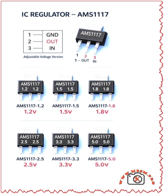
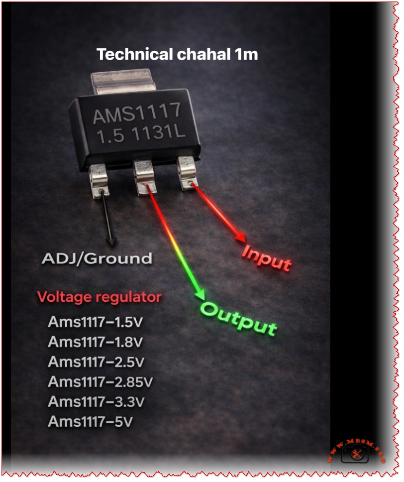
- Simple three‑pin package (GND, OUT, IN) makes board layout straightforward.
- Multiple fixed outputs available: 1.2V, 1.5V, 1.8V, 2.5V, 3.3V, 5.0V.
- Low cost and broad availability for hobby and production use.
- Good for low‑current rails (typical use up to ~1 A with proper thermal design).
Common Mistakes and Corrective Actions
| Common Mistake | Why it Fails | Corrective Action |
|---|---|---|
| No input/output decoupling capacitors | Regulator oscillates or output is noisy | Place recommended capacitors: input 10 µF (electrolytic or tantalum) and output 10 µF low‑ESR close to pins |
| Ignoring thermal dissipation | Device overheats under load; thermal shutdown | Calculate power dissipation ; add heatsink or use switching regulator if W |
| Long traces between caps and pins | Increased ESR/ESL causes instability | Route short, wide traces; place caps within 5 mm of pins |
| Using AMS1117 for high step‑down | Excessive wasted power and heat | Use buck converter for large VIN–VOUT or high current |
| No reverse‑polarity or transient protection | Device destroyed by spikes or reverse connection | Add input TVS diode, series fuse, or reverse‑polarity MOSFET |
| Wrong capacitor type | ESR too high or too low causing instability | Use low‑ESR electrolytic or tantalum on output; ceramic + electrolytic combo on input |
| Expecting full 1 A without thermal design | Device current limit or thermal shutdown | Derate to 0.7–0.8 A unless heatsink and airflow provided |
Practical Design Checklist (Quick Reference)
- Select correct AMS1117 variant for required output voltage (1.2 / 1.5 / 1.8 / 2.5 / 3.3 / 5.0 V).
- Calculate worst‑case dissipation: .
- Choose caps: Input 10 µF low‑ESR; Output 10 µF low‑ESR; add 0.1 µF ceramic for high‑frequency decoupling.
- Thermal plan: Heatsink area, copper pour, and airflow if W.
- Layout: Short traces, wide copper, thermal vias under package for SMD variants.
- Protection: Input TVS, series fuse, reverse‑polarity protection.
- Testing: Thermal imaging under full load; measure output ripple and transient response.
Thermal Calculation Example
- Given: VIN = 12 V, VOUT = 5 V, ILOAD = 0.8 A
- Dissipation:
- Implication: 5.6 W requires substantial heatsinking; AMS1117 in a TO‑220 or SOT‑223 without heatsink will overheat. Consider switching regulator.
Comparison Table: AMS1117 vs. Common Alternatives
| Attribute | AMS1117 (Linear) | LM2596 (Buck) | LDO Modern (e.g., MIC5219) |
|---|---|---|---|
| Efficiency at 5 V out from 12 V in | ~42% | ~85–95% | ~42–60% |
| Typical max current | ~1 A (thermally limited) | 3 A (switching) | 500 mA–1 A |
| Output noise | Low‑mid | Higher switching noise | Low |
| Board complexity | Low | Higher (inductor, diode, caps) | Low |
| Thermal stress | High for large VIN–VOUT | Low | Moderate |
| Best use case | Small loads, simple designs | High current, large step‑down | Low‑noise low‑current rails |
When to Choose AMS1117 (Use Cases)
- Low‑power microcontroller rails (e.g., 3.3 V at < 300 mA).
- Simple sensor boards where VIN is close to VOUT (small voltage drop).
- Prototyping and low‑volume products where cost and simplicity matter.
When to Avoid AMS1117 (Alternatives)
- High current (>1 A) or large VIN–VOUT difference — use a buck converter.
- Battery‑powered designs where efficiency is critical — use switching regulator.
- Very low noise analog rails — choose a precision LDO with low noise spec.
Layout and PCB Best Practices
- Place caps within 2–5 mm of regulator pins.
- Use wide input and output traces (or pour copper) to reduce voltage drop and improve heat spreading.
- Add thermal vias under SMD packages to move heat to inner or bottom copper.
- Keep sensitive analog traces away from the regulator’s hot copper and switching nodes (if present).
- Label polarity clearly and include test points for VIN, VOUT, and GND.
Testing and Validation Steps
- No‑load test: Verify VOUT with no load; check for oscillation.
- Step‑load test: Apply sudden load changes and measure transient response.
- Thermal test: Run at maximum expected load for 30 minutes; measure case and PCB temps.
- Ripple test: Measure output ripple with oscilloscope; ensure within tolerance for your circuit.
- Fault test: Simulate short‑circuit and overvoltage to confirm protection behavior.
Common Failure Modes and Troubleshooting
- Symptom: Output drops under load → Check thermal shutdown, insufficient input voltage, or current limit.
- Symptom: Output noisy or oscillating → Check output capacitor ESR and placement.
- Symptom: Device hot to touch → Check power dissipation calculation and add heatsink or switch to buck converter.
- Symptom: No output → Check input presence, reverse polarity protection, and solder joints.
Engineering Notes and Practical Tips
- Combine capacitors: a 0.1 µF ceramic in parallel with a 10 µF electrolytic gives best high‑ and low‑frequency performance.
- Derate current: assume 70–80% of the absolute max in real designs unless thermal path is proven.
- Use thermal simulation or simple hand calculations to size copper pour and heatsink.
- Document expected VIN range and include transient protection if VIN can spike (e.g., automotive or industrial environments).
Focus Keyphrase
AMS1117 common mistakes thermal design decoupling capacitor layout oscillation protection buck alternative 1.2V 1.8V 3.3V 5V regulator
SEO Title
Mbsmpro.com, AMS1117 Voltage Regulator, Common Mistakes, Thermal Design, 1.2V–5.0V, Decoupling, Layout, Alternatives
Meta Description
Avoid overheating and instability with AMS1117 regulators. Learn the most common mistakes, thermal calculations, capacitor recommendations, PCB layout tips, and when to choose a buck converter instead.
Slug
ams1117-common-mistakes-thermal-design-decap-layout-alternatives
Tags
AMS1117, Voltage Regulator, LDO, Decoupling, Thermal Design, PCB Layout, Buck Converter, 3.3V, 5V, Mbsmgroup, Mbsm.pro, mbsmpro.com, mbsm, Electronics, Power Supply
Excerpt (first 55 words)
AMS1117 linear regulators are simple and cheap, but common mistakes—missing decoupling, poor thermal planning, and long traces—cause instability and overheating. This guide explains capacitor choices, power dissipation math, PCB layout rules, testing steps, and when to switch to a buck converter for efficiency and reliability.